Overview Signal/Power Integrity Checking Service
Major Advantages
- Have improved confidence in your design
- Independant expert advice
- Low cost service
- Highlight any potential problems and give suggested improvements
- No need to own expensive SI/PI tools
- More detailed SI/PI simulation can be performed (additional cost)
Introduction
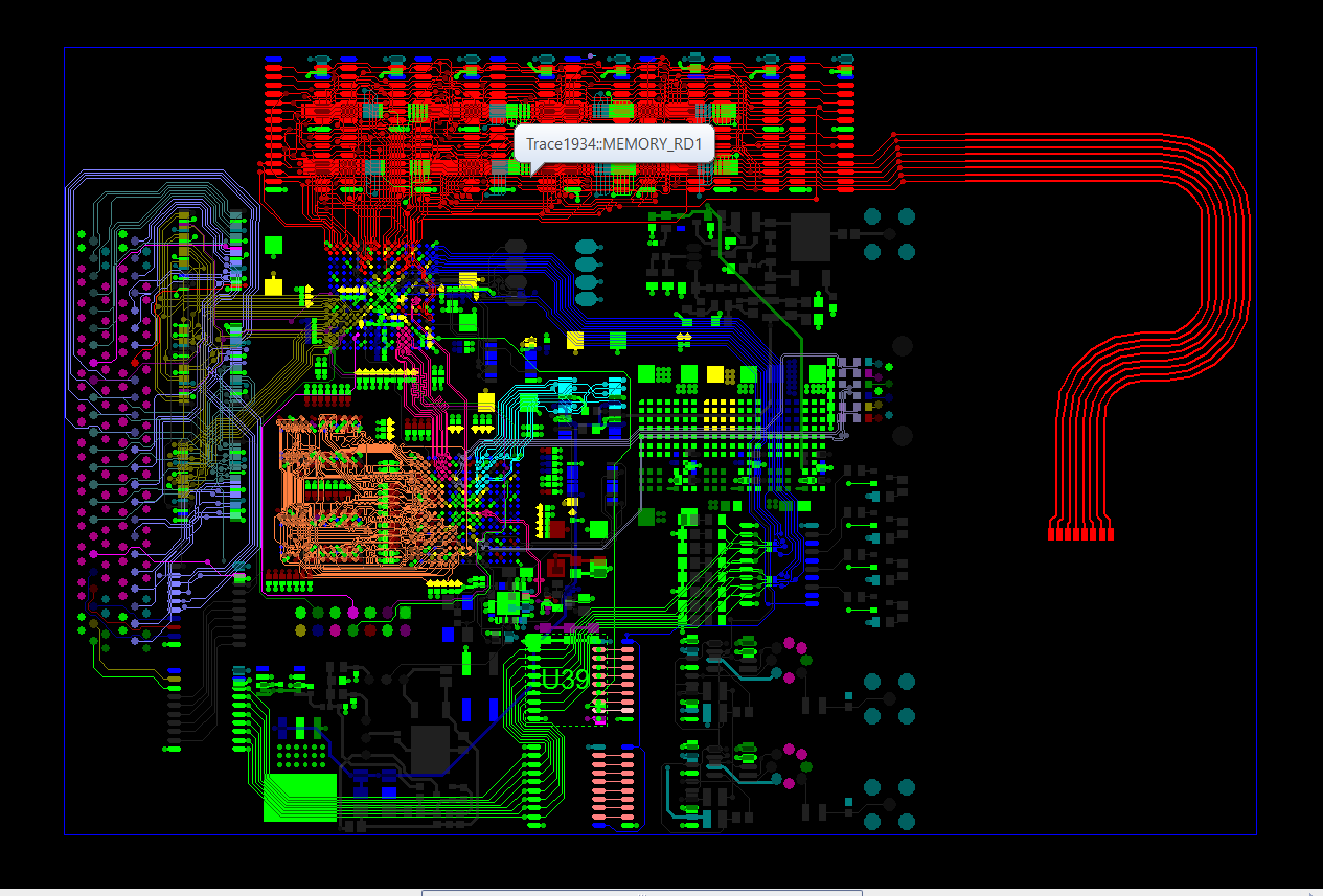
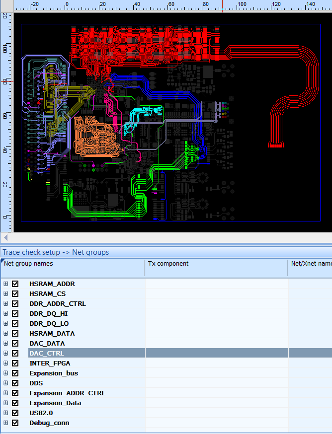
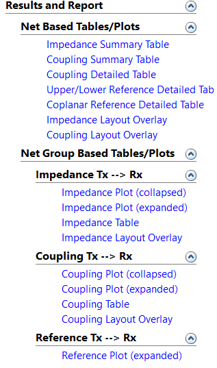
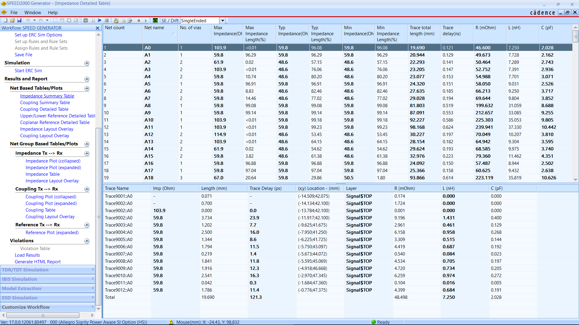
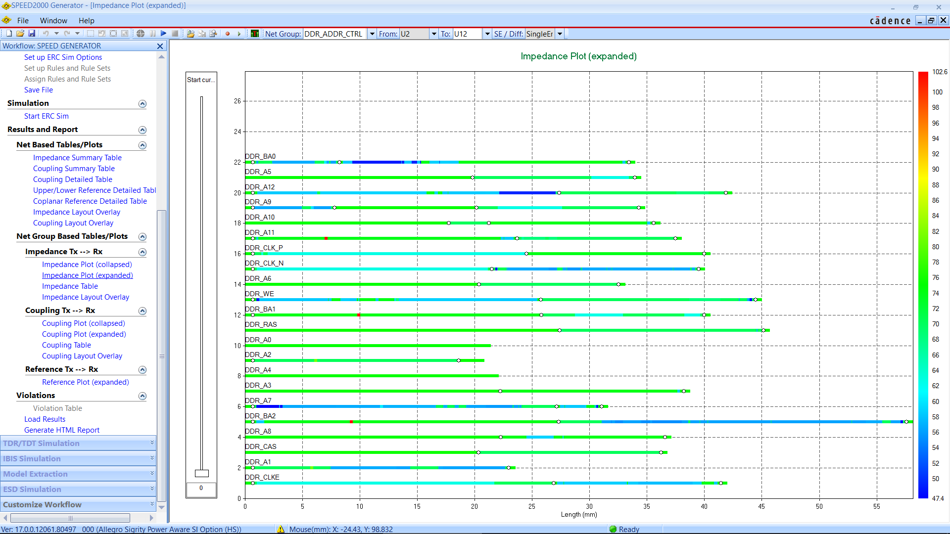
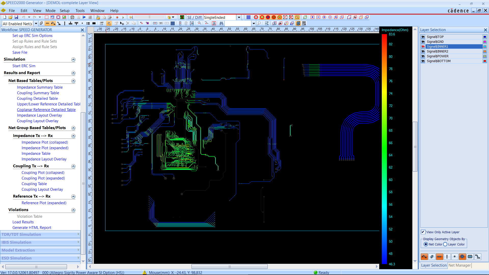
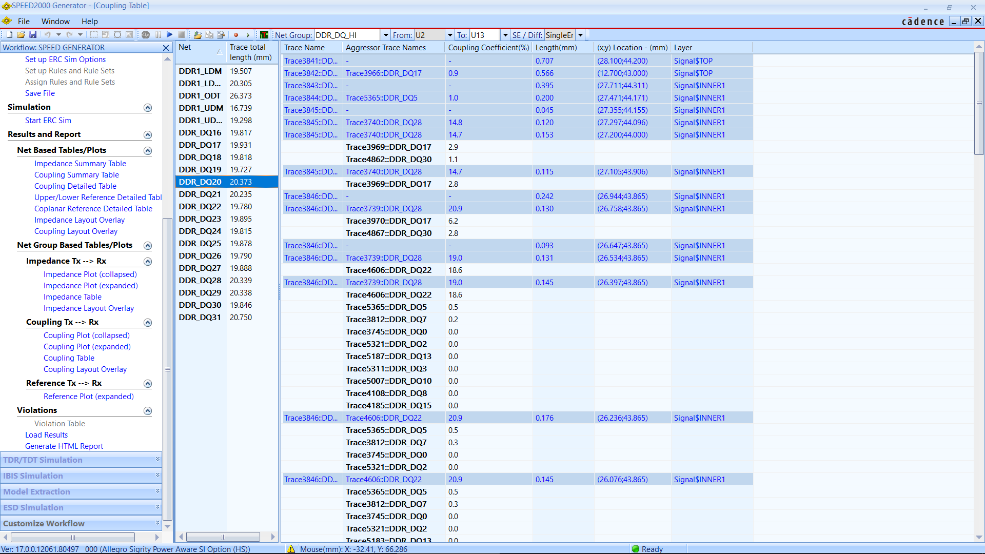
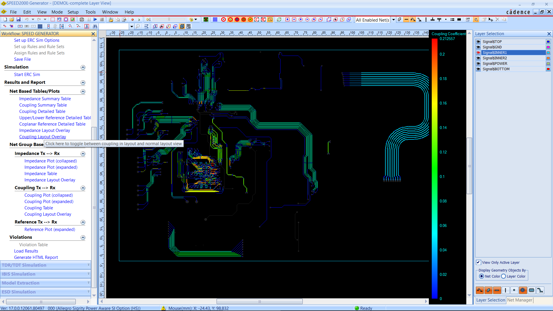
With the Signal/Power Integrity Checking Service our aim is not to run full SI/PI analysis on your design, but rather run a relatively quick health check on the PCB board design to determine if there are areas of concern in the design. Reports report will be generated that give the following details: -
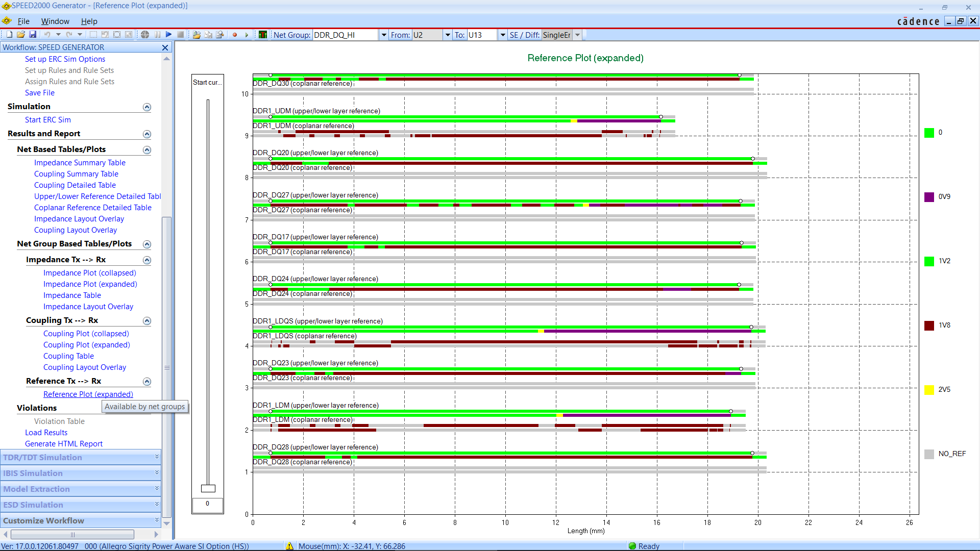
- Trace reference Checking
- Trace reference-aware impedance
- Trace reference-aware coupling (crosstalk)
- Differential pair routing phase
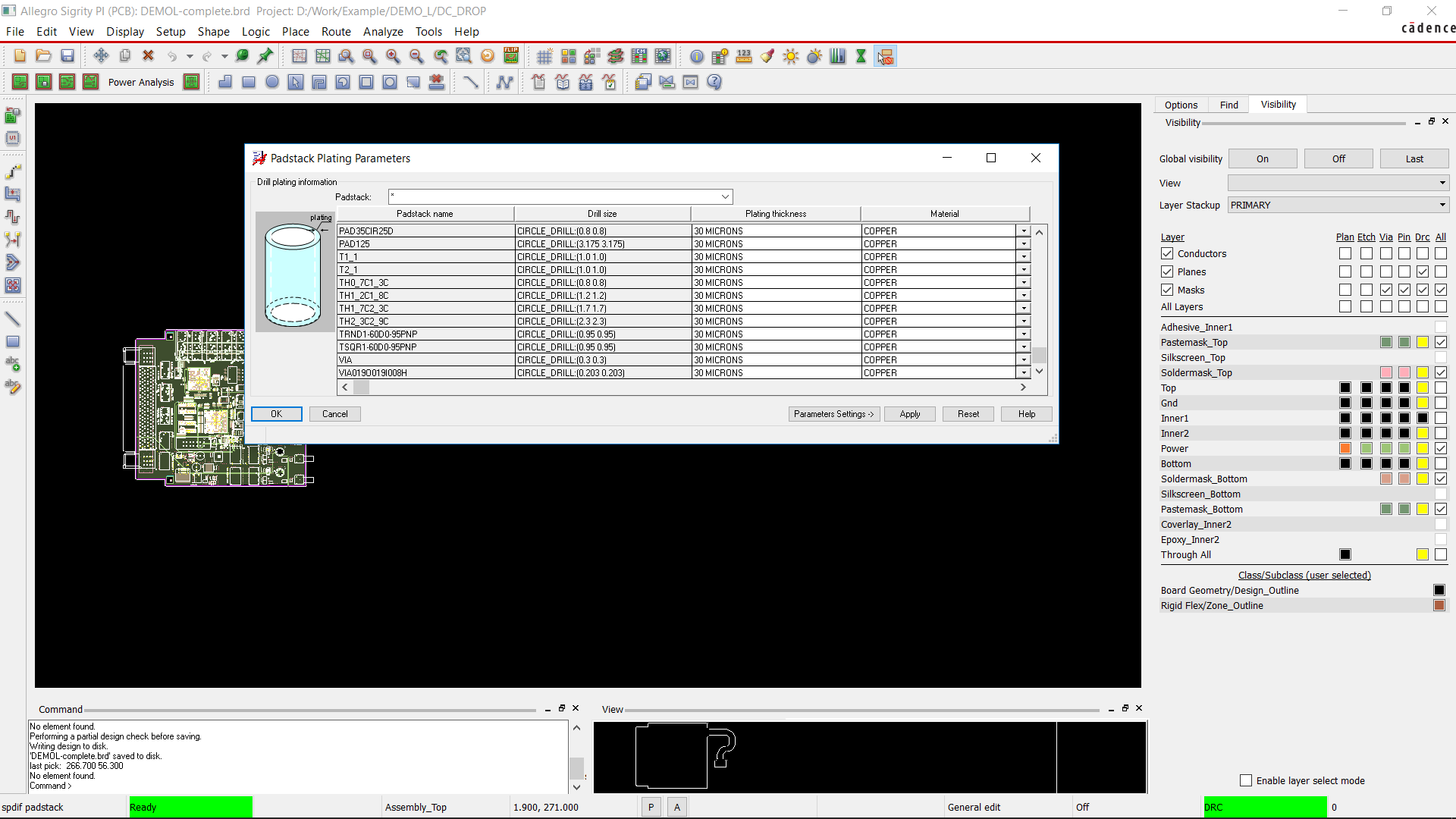
- Number of vias
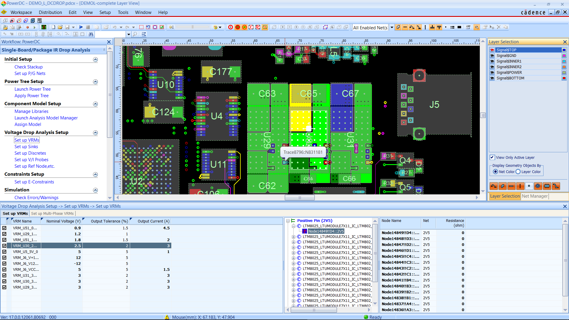
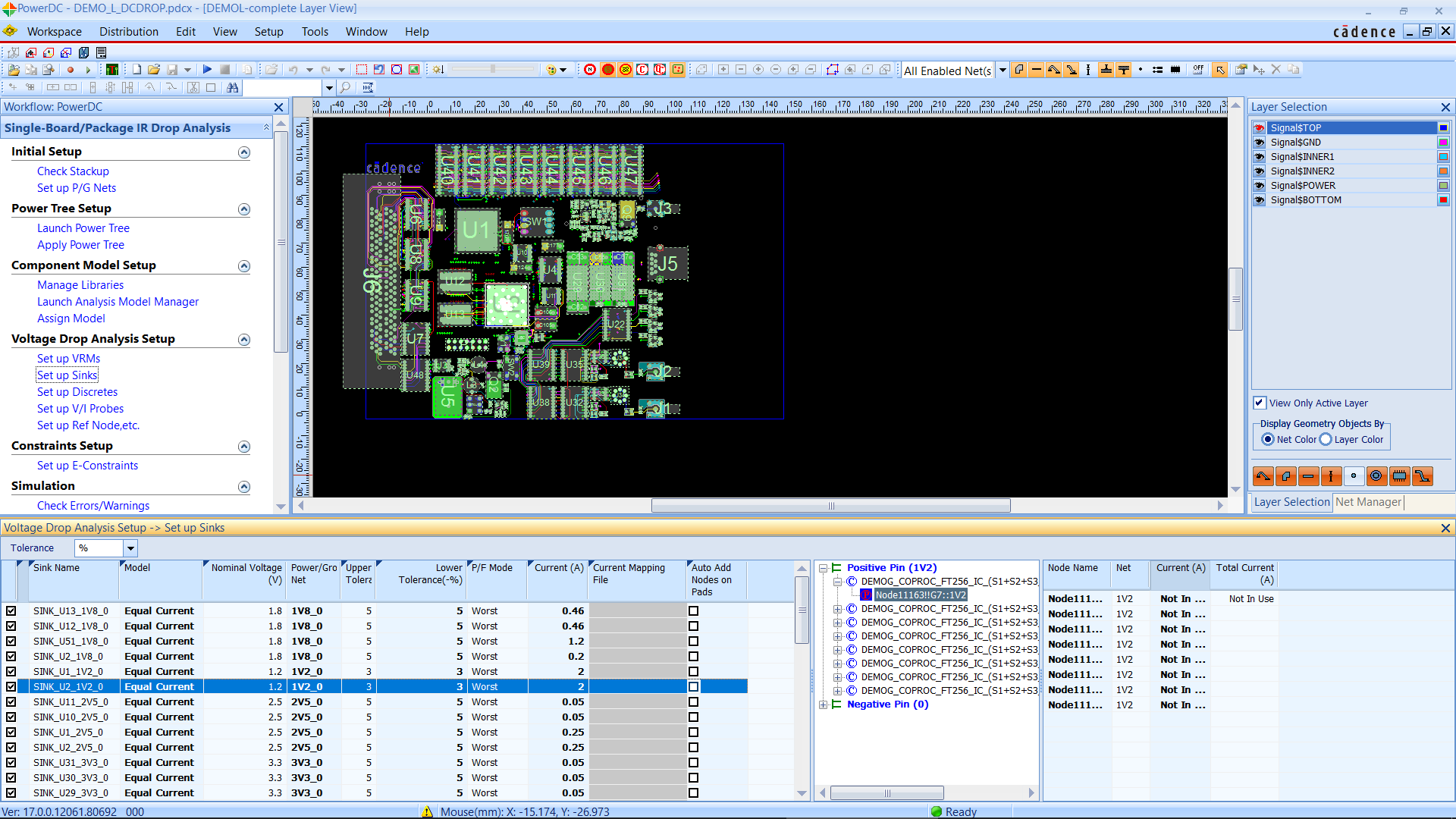
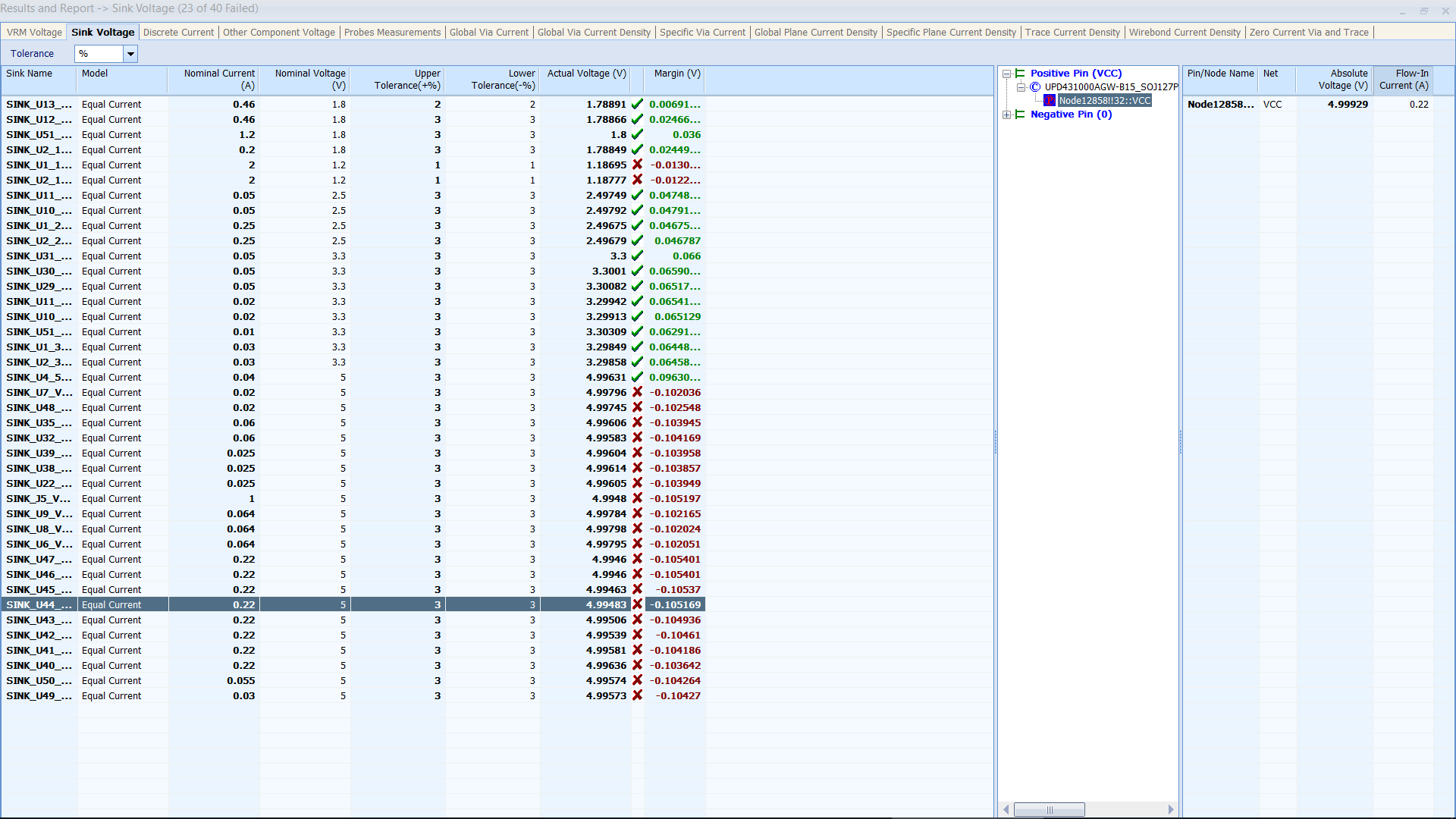
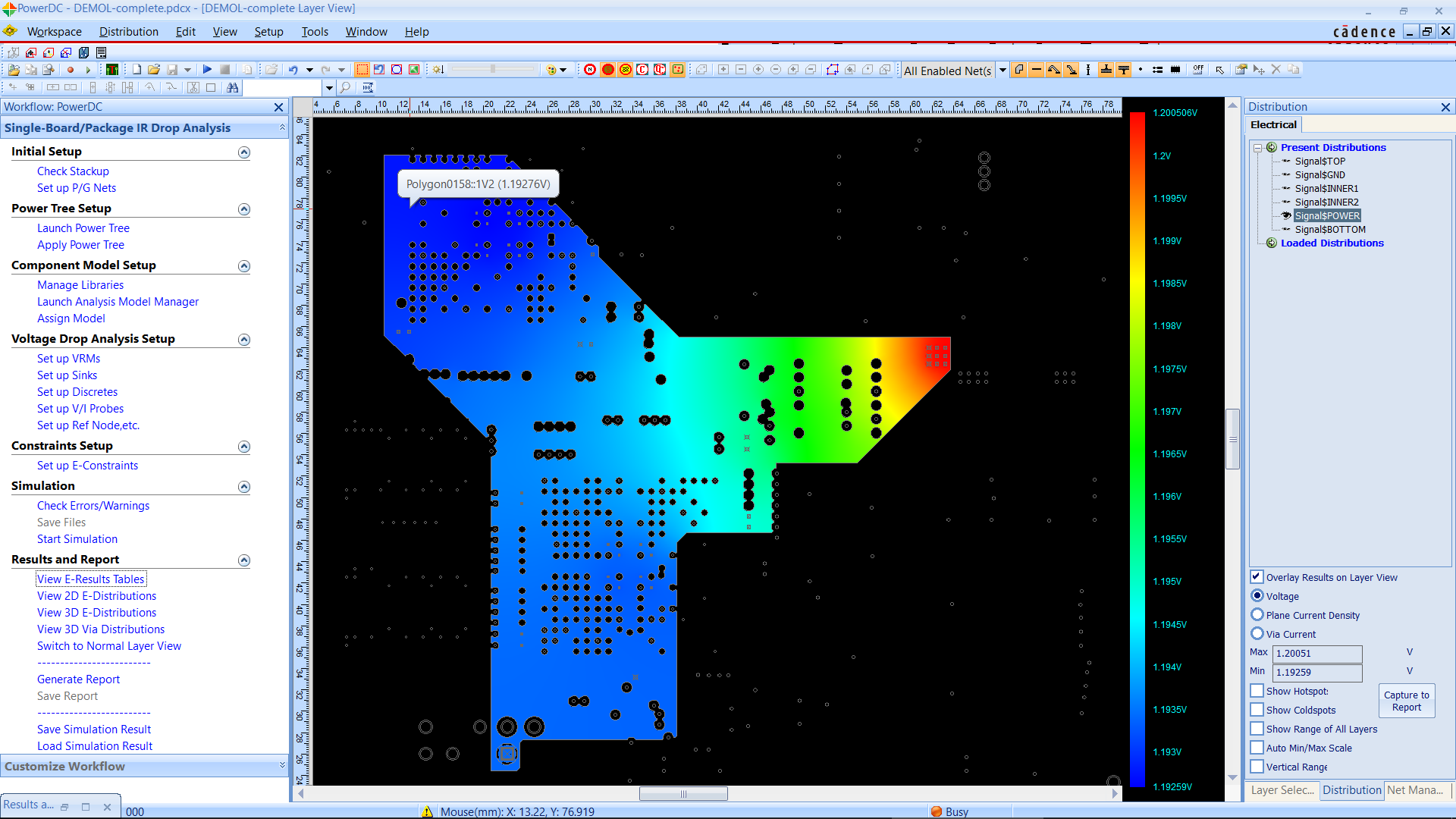
- Supply Voltage Drop
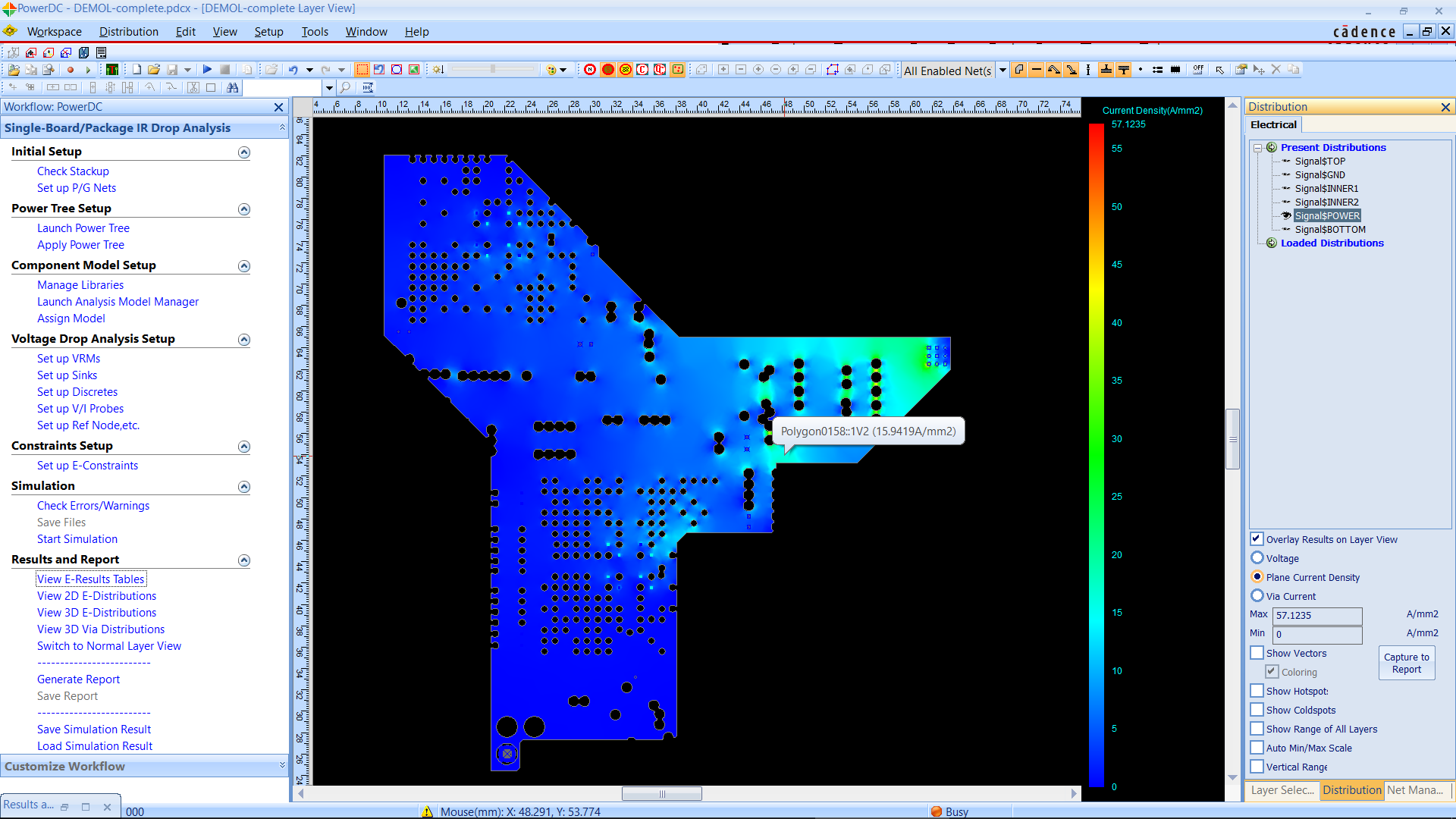
- Power Plane/ Power Trace Current Density
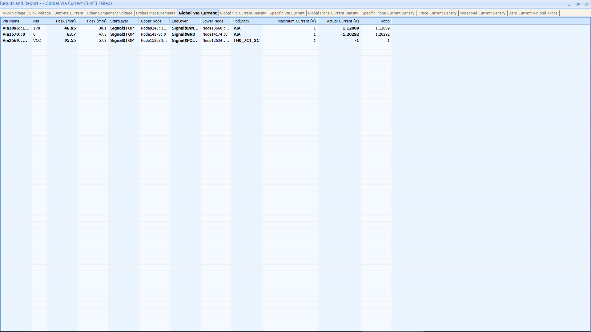
- Power Via Current and Current Density
Based on the simulation results we will make recommendations for improvements in the PCB layout and also if we believe that more in-depth simulations are required. Note that as we are not using IBIS or SPICE models of the drivers and receivers for these simulations as our aim is to give a fast turnaround service that carries out basic checks on a PCB design for impedance, crosstalk, DC Drop and current, current density and the like.